Gan Hemt Process Flow
Ieeexplore Ieee Org Iel7 Pdf
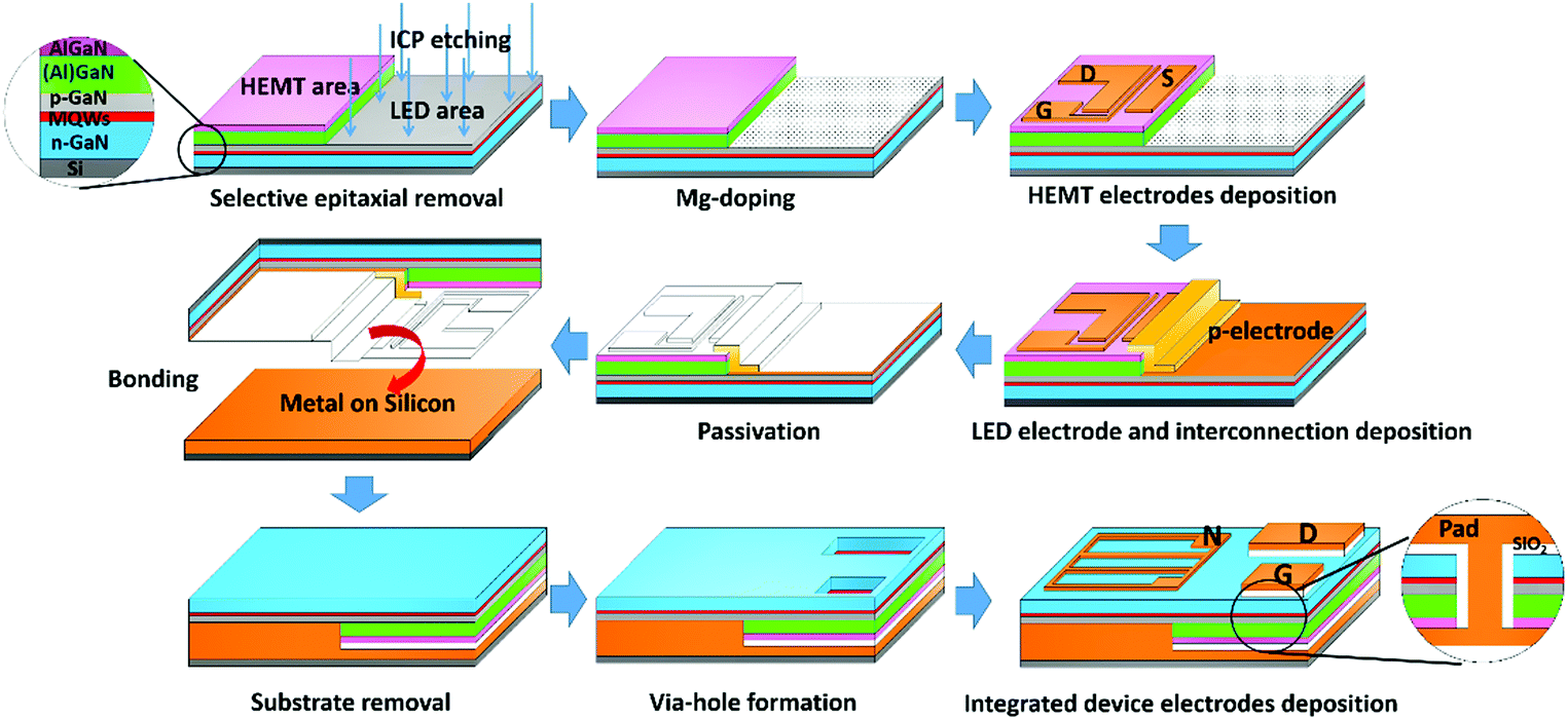
Efficiency Improved By Monolithic Integration Of Hemt With Vertical Structure Leds And Mg Doping On Dry Etched Gan Journal Of Materials Chemistry C Rsc Publishing Doi 10 1039 C9tch

Gold Free Contacts On Alxga1 Gan High Electron Mobility Transistor Structure Grown On A 0 Mm Diameter Si 111 Substrate Journal Of Vacuum Science Technology B Vol 34 No 4
Making Improvements With Multiple Materials News
Electronics Free Full Text A Comprehensive Review Of Recent Progress On Gan High Electron Mobility Transistors Devices Fabrication And Reliability Html
Electronics Free Full Text An Investigation Of Carbon Doping Induced Current Collapse In Gan On Si High Electron Mobility Transistors Html
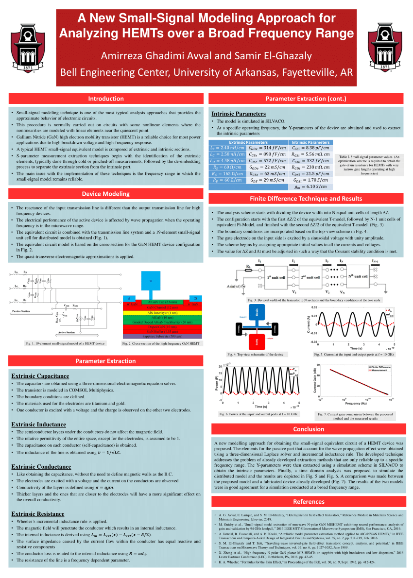
AlGaN/GaN high electron mobility transistors (HEMTs) are good candidates for high power, high frequency, and low loss applications because of high critical breakdown field and high electron mobility 9–14 The breakdown voltage (BV) is one of the most important design targets, and the reported values are still far below the theoretical limit.
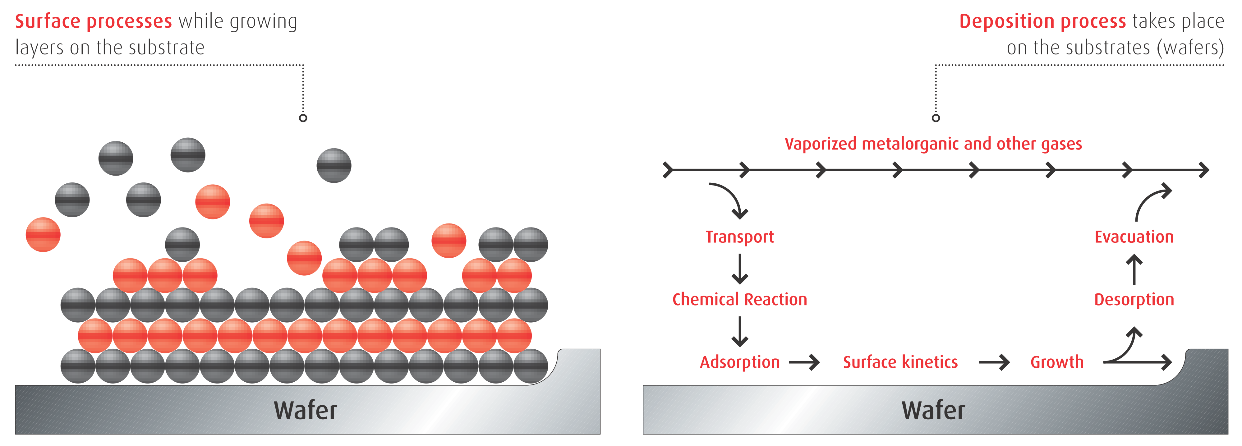
Gan hemt process flow. To illustrate the process, Cree’s SiC device C3MJ (900V, 35A) and GaN Systems’ GaN HEMT GS (900V, 35A) are used in the examples Results of power losses from the Thermal Module are compared with the results from the SPICE simulation 1 Loss Calculation of SiC Devices. Figure 2 (a) Fabrication process flow of monolithic Si–GaN cascode FET (b) Key steps of transfer printing and selfaligned etching technology The SiN cap layer electrically isolated the Sibased transistor from the underlying AlGaN/GaN material in the final cascode device The SiN reduced leakage currents by some nine orders of magnitude. Sink layer for Gallium Nitride (GaN) high electron mobility transistors (HEMTs) The NRL “Gate after diamond” approach has demonstrated % reduction in selfheating The second generation of this process implements diamond directly on GaN to serve both as a passivation layer and to increase the heat spreading effect.
DUBLIN, Feb 22, 17 /PRNewswire/ Research and Markets has announced the addition of the "Transphorm GaN on Si HEMT TPH36PS Technology Analysis" report to their offering Transphorm's TPH36PS transistor has a new die design and manufacturing process The die contacts are optimized on the die area to save space, and increase current density. AlGaN/GaN heterostructure high electron mobility transistors (HEMTs) have attracted considerable attention due to their potential applications in high power and high frequency devices 1–3To enhance the transport properties of twodimensional electrons gas (2DEG) and reduce the leakage current at higher electric fields in HEMTs, an underlying highresistivity carbon doped GaN (CGaN) layer. Fig 2 Process flow for fabricating stretchable AlGaN/GaN HEMTs 3 Fig 3 (a) Fabricated AlGaN/GaN HEMTs in stretchable geometries (b) PostICP etch with exposed Si substrate (c) Wirebonded devices (d) Released AlGaN/GaN HEMT postXeF.
The 025µm GaN HEMT process Process main features GH25 GaN process is optimized for high power amplification up to GHz The power density combined with a thermal dissipative SiC substrate reaches 4W/mm This MMIC process includes MIM capacitors, inductors, air bridges, metallic resistors, via through the substrate and two metal layers for. AlGaN/GaN high electron mobility transistors (HEMTs) are good candidates for high power, high frequency, and low loss applications because of high critical breakdown field and high electron mobility 9–14 The breakdown voltage (BV) is one of the most important design targets, and the reported values are still far below the theoretical limit. A GaNonSapphire HEMT Process Flow Example ③Deposit S/D metal Ø Deposit ohmic contacts on top of AlGaN as source and drain Sapphire Substrate Buffer GaN AlGaN S D ④Liftoff and Anneal Ø To improve contact quality Ø Bad annealing may dramatically degrade the device performance ⑤Mask 03 –Gate Ø Definegateregion Ø Thealignmentinthisstepis.
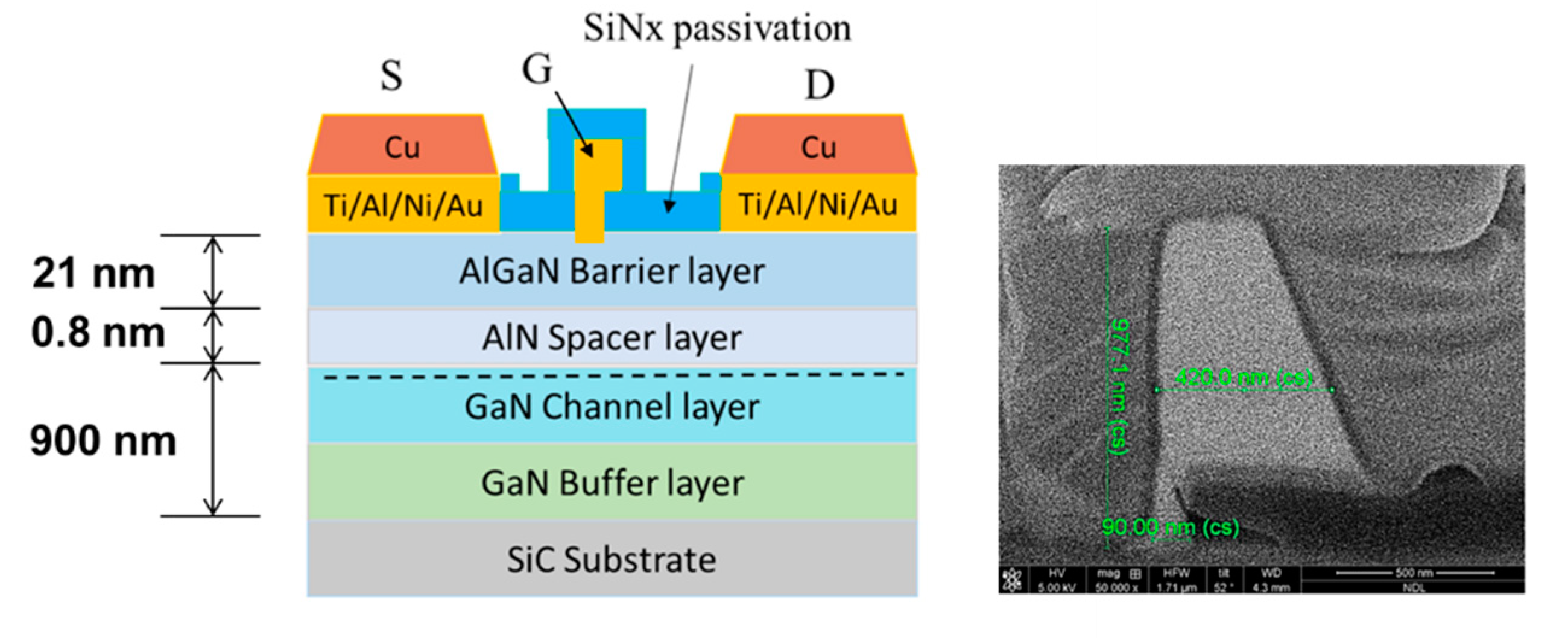
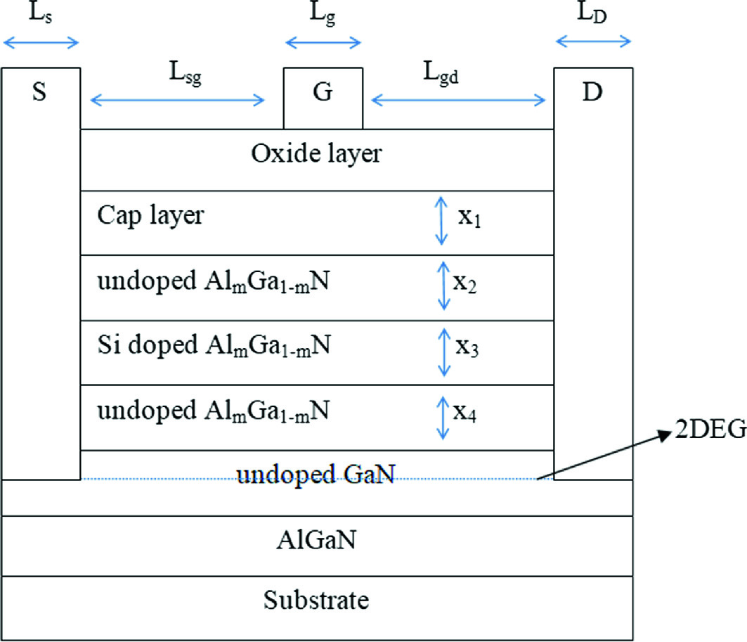
Power High High complex fabrication process flow of HEMT device in Consumption simpler way that will be used at high power 6 more reliable than BJTsAlGaN/GaN high electron mobility transistors (AlGaN/GaN HEMTs) can be I INTRODUCTION used for high frequency, highpower and high temperature applications because of their wide band A HEMT. Figure 6 Process flow for the fabrication of PCMenabled GaN high electron mobility transistors (HEMTs) The top AlGaN layer had a thickness of 25 nm and the GaN buffer was 18 μm thick, while the 550 μm thick Si substratehad a (111) orientation. AlGaN/GaNonSiC HEMTs • Low and high anneal temperature ohmic metal processes for GaNbased transistors have been tested for buffer leakage • Improvements in maximum achievable voltage for the low temperature process • Higher power will be achievable with such a contact compared to the conventional process.
GaN HEMT/Si( C ) P(M)HEMT/GaAs Process Roadmaps D004GH OMMIC Innovating with IIIV’s 02/04/15 7 100nm et 60nm GaN HEMTs to replace GaAs PHEMTs thanks to MMIC « PROCESS FLOW « AlGaN/GaN/Si OMMIC Innovating with IIIV’s 02/04/15 11 OMMIC CONFIDENTIAL 15 Lg = 100 nm 0 100 0 300 400 500 600 700 800 900 0 5 10 15 25 30 Vds. Fig 3 Standard GaN/Diamond HEMT s process Flow Using a standard GaN/SiC HEMT s process procedure, 05 um Ga N/Diamond HEMTs was fabricated with high temperature o hmic alloying,. PhysicsBased MultiBias RF LargeSignal GaN HEMT Modeling and Parameter Extraction Flow Abstract In this paper, a consistent DC to RF modeling solution for Al gallium nitride (GaN)/GaN high electron mobility transistors is demonstrated that is constructed around a surfacepotentialbased core.
Fig 1 a Schematic cross section and dimensions of the HEMTs b Device fabrication process flow Tzou et al Nanoscale Research Letters (17) Page 2 of 6 AlN. Growth of AlGaN/GaN heterojunction layers in the MOCVD process However, we have lacked the ability to add dopants (in particular, ptype) to this process to grow a layer of PGaN Therefore, our MOCVDbased GaN HEMTs that SNF could make were depletionmode devices However, now we have a PGaN recipe for LEDs in SNF We. The report also proposes a comparison with the GaN Systems GSB 650V HEMT This comparison highlights the huge differences in design and manufacturing process and their impact on device size.
Improving Transport Properties of GaNBased HEMT on Si (111) by Controlling SiH 4 Flow Rate of the SiN x NanoMask JinJi Dai 1,2 , ChengWei Liu 1 , SsuKuan Wu 1 , SaHoang Huynh 1 , JhenGang Jiang 1 , SuiAn Yen 1 ,. Process flow for fabrication of protected and passivated AlN/GaN MOSHEMTs using the gate wraparound technique Processing includes (a) sample cleaning and deoxidation, (b) 2 nm Al deposition, (c) etching Ohmic regions and thermal oxidation of Al, (d) Ohmic metallisation and annealing, and (e) gate metallisation and device measurements. The report also proposes a comparison with the GaN Systems GSB 650V HEMT This comparison highlights the huge differences in design and manufacturing process and their impact on device size.
Growth of AlGaN/GaN heterojunction layers in the MOCVD process However, we have lacked the ability to add dopants (in particular, ptype) to this process to grow a layer of PGaN Therefore, our MOCVDbased GaN HEMTs that SNF could make were depletionmode devices However, now we have a PGaN recipe for LEDs in SNF We. The GaN HEMT utilizes highdensity twodimensional electron gas (2DEG) accumulated in the boundary layer between GaN and AlGaN through their piezoelectric effect and natural polarization effect This makes it possible to realize a low onstate resistance (R on). Critical process steps We discuss optimizing the backside via process to eliminate pillar formation during SiC and GaN dry etching for GaN HEMT fabrication Details of subsequent post etch cleaning to reduce byproducts is also discussed The overview of the process flow is shown in Figure 1 All etching was.
The selective ICP etching of GaN against AlGaN was studied to form the ptype GaN gate on the Al 025 GaN/GaN HEMT The ICP etching was employed with the ICP and bias powers of 1 and 7 W, respectively, using Cl 2 and Ar gases with flow rates of and 5 sccm, respectively. Ideal for 5G wireless infrastructure and radar applications (PA and switches) 15, 28, and 48V PA operations. AlGaN/GaN high electron mobility transistors (HEMTs) stand out with superb advantages for highpower, hightemperature, highfrequency applications These issues were overcome when the successful implementation of uniaxial stress in the CMOS process flow was achieved in the early 00s the 90 nm node 22 Longitudinal tensile stress was.
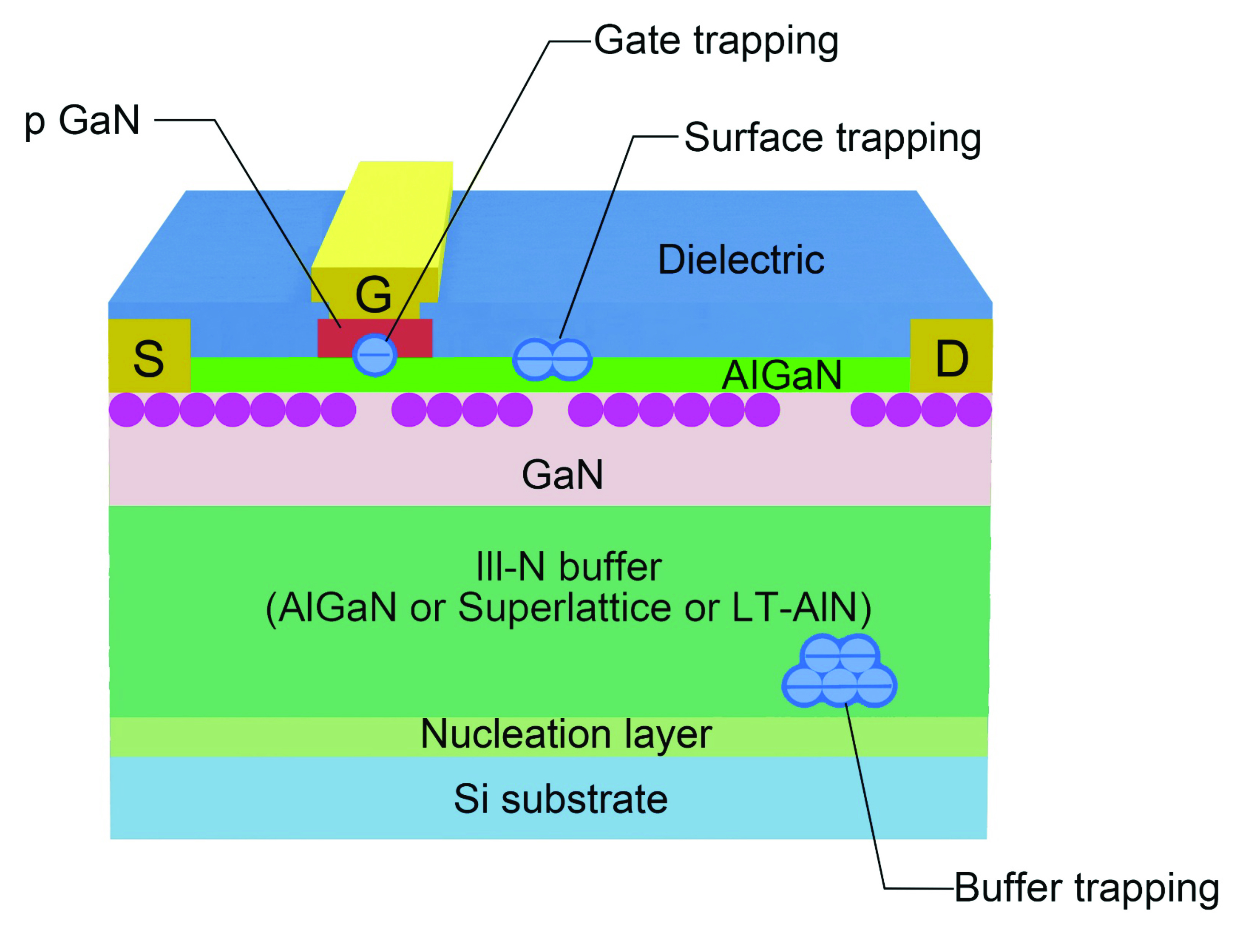
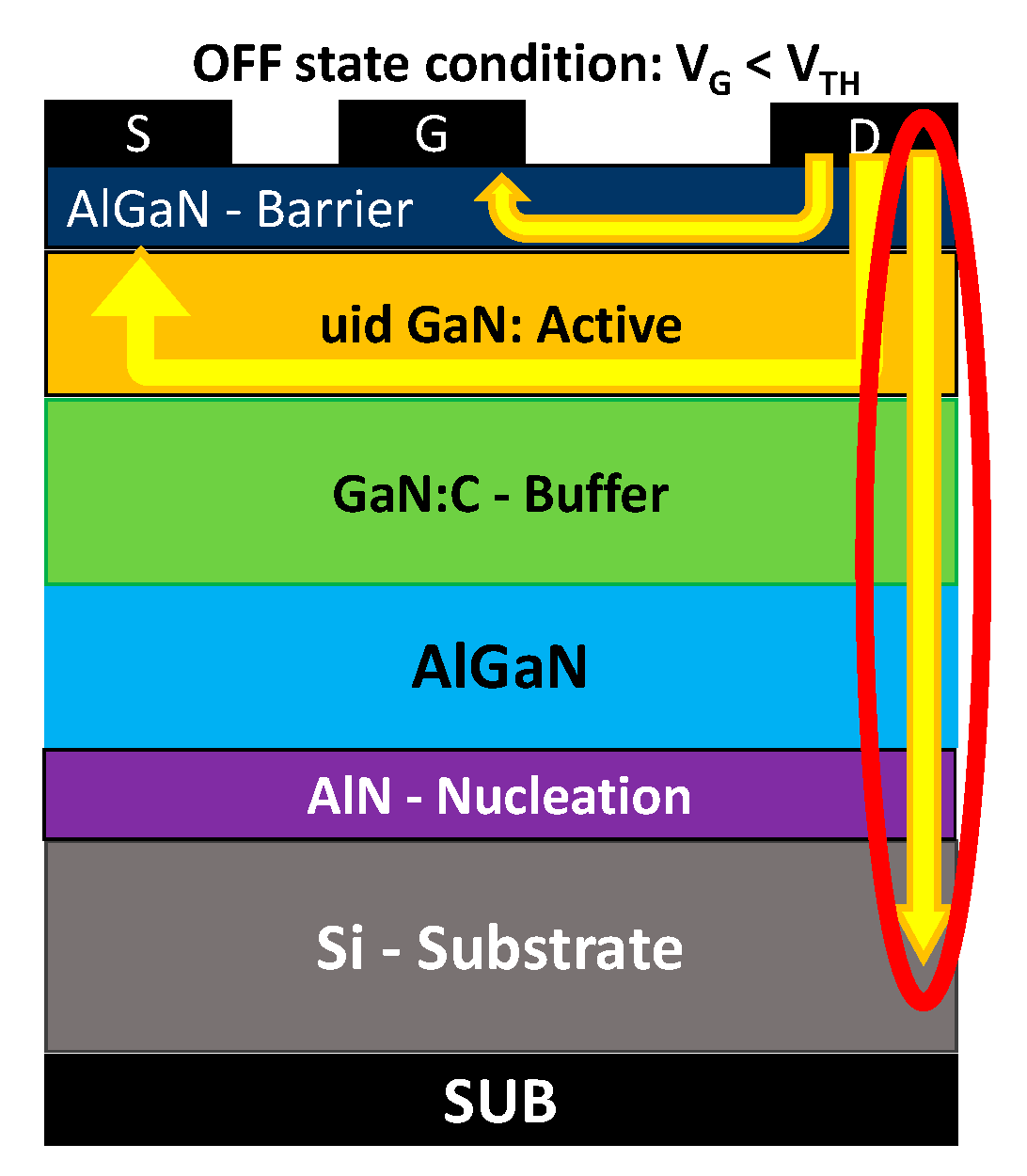
TCADbased Model Extraction Flow for GaN HEMT Devices This webinar will present a model parameter extraction methodology for GaN HEMT devices This will include a review of the current SPICE compact models for GaN HEMT devices, with a discussion of VerilogA and simulator builtin models. AlGaN/GaNonSiC HEMTs • Low and high anneal temperature ohmic metal processes for GaNbased transistors have been tested for buffer leakage • Improvements in maximum achievable voltage for the low temperature process • Higher power will be achievable with such a contact compared to the conventional process. The same effect on normally‐on HEMTs without gate dielectric is possible In the representative case reported in , the trapped charge is located in the semiconductor epilayers eg the AlGaN barrier and the trapping is promoted by high gate–drain electric fieldA positive or negative threshold shift during operation may be critical in the design of the gate driver, since it may cause.
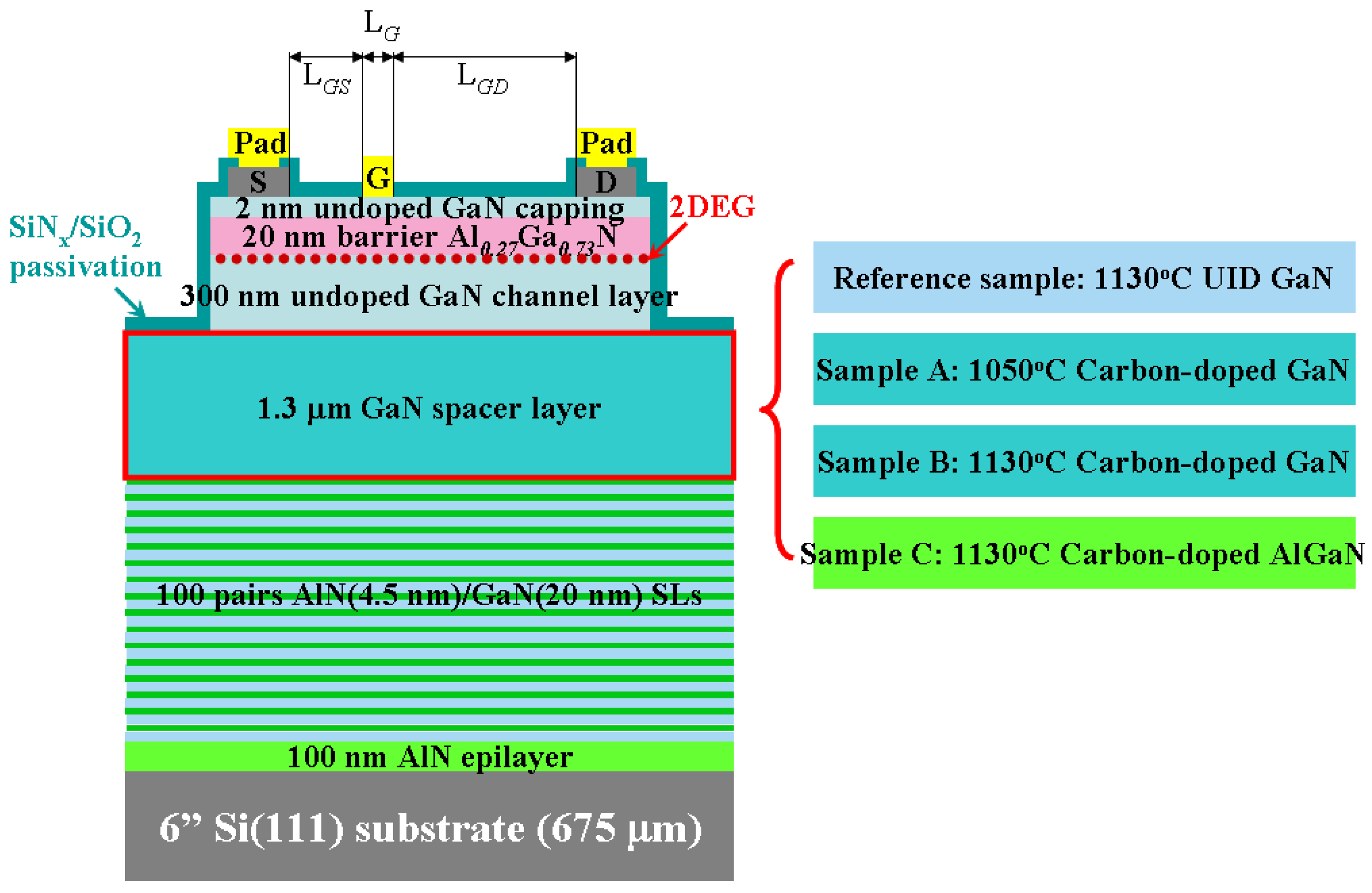
As a first attempt at fabricating AlGaN/GaN HEMTs at RIT, a basic process flow was developed Fig 5 shows the process flow in terms of the cross sections The initial substrate supplied had a 2nm UIDGaN cap, with 25nm of Al 027 Ga 073 N below, GaN with several buffer layers The first step in the process flow designed was the mesa isolation. GaN Technology for High Frequency Applications • Agenda – Brief MACOM History – Winning in the Marketplace – Why GaN – GaN HEMT Structure – High Frequency/High Power Applications – GaN/SiC vs GaN/Si – GaN vs Alternate Technologies – GaN Challenges • Design • Process • Reliability – Future Directions – Summary 2. Nexperia has released the GANWSA, its first GaN AECQ101 power device!.
High Etch Selectivity of GaN over AlGaN 0 Samco solved the selectivity issue by using a small flow of an additive gas (“Gas X”) in a chlorinebased gas plasma mixture An etch selectivity of 601 (GaN/AlGaN) is achieved, and the etch process is successfully stopped on the AlGaN interface without overetching. Affect their process and are suitable to the processing flow After the usual wafer cleaning and inspection, an epitaxial layer must be grown to provide the required material characteristics necessary for HEMT and PHEMT devices The process starts with a GaAs buffer layer epitaxially grown to isolate defects from the substrate and provide a. Improving Transport Properties of GaNBased HEMT on Si (111) by Controlling SiH 4 Flow Rate of the SiN x NanoMask JinJi Dai 1,2 , ChengWei Liu 1 , SsuKuan Wu 1 , SaHoang Huynh 1 , JhenGang Jiang 1 , SuiAn Yen 1 ,.
Power High High complex fabrication process flow of HEMT device in Consumption simpler way that will be used at high power 6 more reliable than BJTsAlGaN/GaN high electron mobility transistors (AlGaN/GaN HEMTs) can be I INTRODUCTION used for high frequency, highpower and high temperature applications because of their wide band A HEMT. Fig 3 Flow chart of GaN HEMT fabrication process including field plate step After the passivation maximum current density was 1100 mA/mm and maximum extrinsic transconductance, g m was 260 mS/mm After this step, electron beam lithography is used to define the field plate regions and these regions were deposited with Ti/Au metals. The TPH3002PS is a 600V EZGaN™HEMT for high frequency operations from Transphorm Manufactured by Fujitsu and assembled in a TO2 package, it features the QuietTabTM scheme which increases switching speed by 0% With a 75ns turnon and a 10ns turn off, the TPH3002PS has a higher switch frequency than the best CoolMOS.
AlGaN/GaN Lateral HEMT Devices • AlGaN/GaN High Electron Mobility Transistors feature –Low Ron due to high 2DEG density 12with n s ~9x10 cm2 and high mobility (~00 cm2/Vs) –High breakdown because of high bandgap (34 eV) –Low capacitance no junctions to deplete (undoped) Si High mob GaN S D Source Gate Drain GaN Al Ga N x 1x P. GaN processes and applications Power electronics Replacement of SI solutions Si to improve the DC efficiency of DC power converters Switching Transistors Schottky Diodes RF Transistors and MMICs 05µm and 025µm HEMTs to replace high power LDMOS ( > 100W) 100nm et 60nm GaN HEMTs to replace GaAs PHEMTs thanks to. Figure 6 shows the process flow of the devicetransfer GaNonDiamond HEMT In this last context, the transfer of high electron mobility transistors (HEMTs) on diamond substrates represents an.
The GANWSA is a 650 V, 50 mΩ Gallium Nitride (GaN) FET It is based on a cascode configuration of a GaNonsilicon High Electron Mobility Transistor (HEMT) to handle high voltages and a standard low voltage silicon Metal Oxide Semiconductor Field Effect Transistor (MOSFET). 13 IEEE Compound Semiconductor Integrated Circuit Symposium (CSICS) We report on a novel fabrication process of GaNonDiamond high electron mobility transistors (HEMTs) and its resulting thermal performance enhancement over conventional GaNonSiC technology In this process, GaN devices are first fabricated on their epitaxial substrate (eg sapphire or SiC) before being removed from the original substrate and bonded onto a highthermalconductivity diamond substrate at low temperature. Currently GaN high electron mobility transistor (HEMT) technology is under extensive research in both industry and institutes Tinggi Technologies started to development its own HEMT process from 05 This paper evaluates the development of GaN HEMT in past 15 years and the entire fabrication process of Tinggi top GaN HEMT.
We demonstrate the electrical performances of an AlGaN/GaN metal–insulator–semiconductor high electron mobility transistor (MISHEMT) with low gate leakage current (I g)A low gate leakage current as low as the order of 10 −11 A/mm was achieved from normallyoff MISHEMT device (V th = 216 V) with a partially recessed gate, fluorine treatment, and ALD Al 2 O 3 gate dielectric layer. •Overview of GaN HEMT Process and Device Simulation •Compact Modeling Standardization Effort two standard models (ASM, MVSG) •GaN HEMT Model Extraction for Symmetric and Asymmetric Devices •The MVSG model has a good geometry scalability in fitting devices with different gate lengths •TCAD simulations provides a unique approach to separate the extraction of temperature. To illustrate the process, Cree’s SiC device C3MJ (900V, 35A) and GaN Systems’ GaN HEMT GS (900V, 35A) are used in the examples Results of power losses from the Thermal Module are compared with the results from the SPICE simulation 1 Loss Calculation of SiC Devices.
A Combination of high power density, high efficiency, and wide bandwidth ;. GaN Technology for High Frequency Applications • Agenda – Brief MACOM History – Winning in the Marketplace – Why GaN – GaN HEMT Structure – High Frequency/High Power Applications – GaN/SiC vs GaN/Si – GaN vs Alternate Technologies – GaN Challenges • Design • Process • Reliability – Future Directions – Summary 2. TCADbased Model Extraction Flow for GaN HEMT Devices This webinar will present a model parameter extraction methodology for GaN HEMT devices This will include a review of the current SPICE compact models for GaN HEMT devices, with a discussion of VerilogA and simulator builtin models.
We demonstrate the electrical performances of an AlGaN/GaN metal–insulator–semiconductor high electron mobility transistor (MISHEMT) with low gate leakage current (I g)A low gate leakage current as low as the order of 10 −11 A/mm was achieved from normallyoff MISHEMT device (V th = 216 V) with a partially recessed gate, fluorine treatment, and ALD Al 2 O 3 gate dielectric layer. As a first attempt at fabricating AlGaN/GaN HEMTs at RIT, a basic process flow was developed Fig 5 shows the process flow in terms of the cross sections The initial substrate supplied had a 2nm UIDGaN cap, with 25nm of Al 027 Ga 073 N below, GaN with several buffer layers The first step in the process flow designed was the mesa isolation. DUBLIN, Feb 22, 17 /PRNewswire/ Research and Markets has announced the addition of the "Transphorm GaN on Si HEMT TPH36PS Technology Analysis" report to their offering Transphorm's TPH36PS transistor has a new die design and manufacturing process The die contacts are optimized on the die area to save space, and increase current density.
Abstract— A first attempt at fabricating AlGaN/GaN High Electron Mobility Transistors (HEMTs)on a Si substrate was made at RIT A basic process flow was developed to fabricate enhancementmode devices The proposedfabrication flow was attempted and completed The single metallization step using Ni as. Fig 3 Flow chart of GaN HEMT fabrication process including field plate step After the passivation maximum current density was 1100 mA/mm and maximum extrinsic transconductance, g m was 260 mS/mm After this step, electron beam lithography is used to define the field plate regions and these regions were deposited with Ti/Au metals. Detailed optical and Scanning Electron Microscope pictures and crosssections with EnergyDispersive Xray analysis are included to reveal MACOM’s technical choices at the microscopic level of the GaNonSi HEMT and the passive input match dies.
HEMT (High Electron Mobility Transistor) gallium nitride (GaN) transistors first started appearing in about 04 with depletionmode RF transistors made by Eudyna Corporation in Japan Using GaN on silicon carbide (SiC) substrates, Eudyna successfully brought into production transistors designed for the RF market 3. 421 The successful HEMT fabrication depends on the development of the individual process steps (Ohmic contact, Schottky contact, and controlled, selective and anisotropic etch for GaN/AlGaN) to optimize the HEMT characteristics The complete process development is also undertaken this year 43 Timelines. Manufacturing Process Flow •Overview •GaN HEMT Process Flow •Resistor Process Flow •MOSFET Process Flow •Wafer Fabrication Units •Packaging Process Flow Cost Analysis •Main steps of economic analysis •Yields Hypotheses •GaN HEMT FrontEnd & BackEnd.
A bias of 300 V, 55 % of RF power, 40 % of SiCl4 flow, and 3035 mT of pressure * Try to etch until slightly above 2DEG depth * Every time when use master RIE, clean the chamber mechanically If it was used for metal etching even once, it does not etch GaN materials properly Dip sample in HClDI water (12) for 30 s. Currently GaN high electron mobility transistor (HEMT) technology is under extensive research in both industry and institutes Tinggi Technologies started to development its own HEMT process from 05 This paper evaluates the development of GaN HEMT in past 15 years and the entire fabrication process of Tinggi top GaN HEMT. Fig 2 Process flow for fabricating stretchable AlGaN/GaN HEMTs 3 Fig 3 (a) Fabricated AlGaN/GaN HEMTs in stretchable geometries (b) PostICP etch with exposed Si substrate (c) Wirebonded devices (d) Released AlGaN/GaN HEMT postXeF.
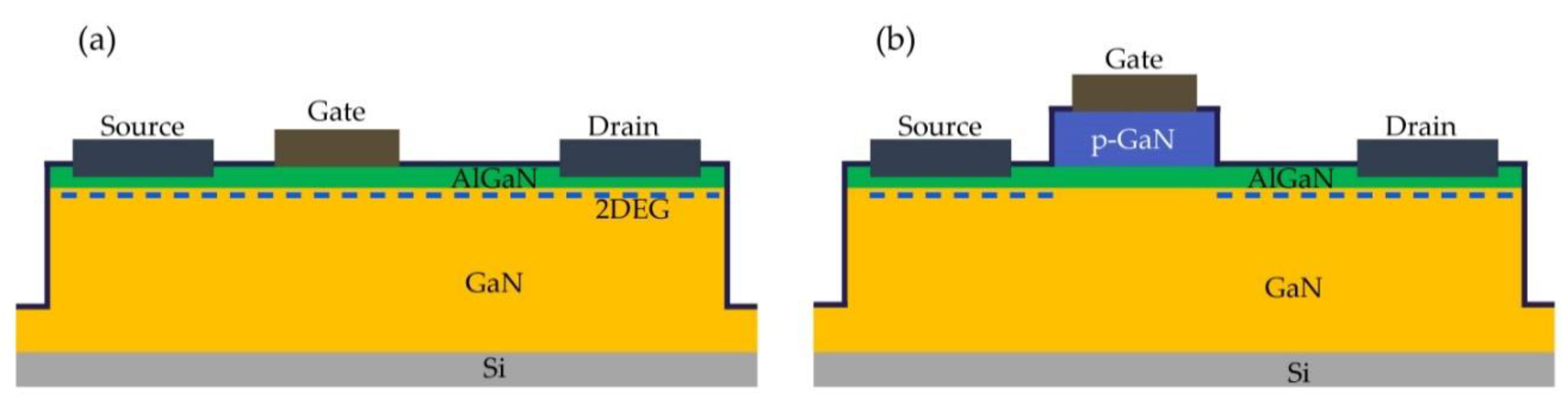
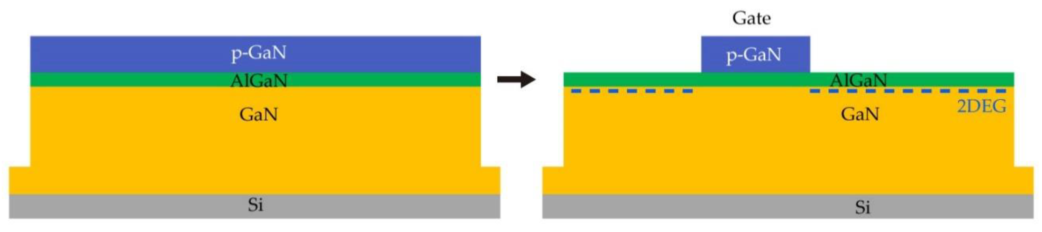
The article presents the results of development of selective etching of pGaN over Al 025 Ga 075 N in Cl 2 /Ar/O 2 ICP plasma for fabrication of normallyoff pGaN gate GaN HEMTs using a laser reflectometry system for precise control of the etched material thickness By optimizing etching process parameters such as oxygen flow, ICP power and chamber pressure, high etching selectivity of p. This process of growing 2Deg will stop when the Fermi levels of both materials will align with each other Fig 34 Energy band of an ndoped AlGaN connecting to GaN showing different Fermi layers and electron flow to the GaN material (left), whole energy band of an ndoped AlGaN/GaN heterostructure after equalizing of Fermi levels showing the.
Www Systemplus Fr Wp Content Uploads 07 Sp563 Innoscience E2 80 99s 650v Gan On Si Transistor Sample Pdf
Www Osti Gov Servlets Purl
Stars Library Ucf Edu Cgi Viewcontent Cgi Article 7690 Context Etd
Revisiting The Seminal Apa Optics Gan Hemt Patent Techinsights

Atomic Layer Deposition Of Gallium Oxide Films As Gate Dielectrics In Algan Gan Metal Oxide Semiconductor High Electron Mobility Transistors Topic Of Research Paper In Nano Technology Download Scholarly Article Pdf And Read For Free On Cyberleninka
Djena Engineering Cornell Edu Papers 14 Ted14 Bo Fringing Cap Gan Hemts Pdf
Micromachines Free Full Text Novel High Energy Efficiency Algan Gan Hemt With High Gate And Multi Recessed Buffer Html

Functionalized Gan Based Transistors For Biosensing Intechopen
Micromachines Free Full Text Gallium Nitride Gan High Electron Mobility Transistors With Thick Copper Metallization Featuring A Power Density Of 8 2 W Mm For Ka Band Applications Html
Snfexfab Stanford Edu Sites G Files Sbiybj8726 F Sections Diplayfiles Engr241 Final Report Sj Al 1819win Pdf
Aip Scitation Org Doi Am Pdf 10 1063 1 Class Chorus Notvisible
Http Www Semiconductor Today Com Features Pdf Semiconductor Today April May 16 Vertical Cmos Pdf
Micromachines Free Full Text A Novel Gan Metal Insulator Semiconductor High Electron Mobility Transistor Featuring Vertical Gate Structure Html
Iopscience Iop Org Article 10 10 1361 6463 af9d Pdf

Process Flow Of The Gate Last Self Aligned Process Download Scientific Diagram
Materials Free Full Text An Overview Of Normally Off Gan Based High Electron Mobility Transistors Html
2

A Review Of Silicon Based Wafer Bonding Processes An Approach To Realize The Monolithic Integration Of Si Cmos And Iii V On Si Wafers
Groove Type Channel Enhancement Mode Algan Gan Mis Hemt With Combined Polar And Nonpolar Algan Gan Heterostructures
Nanoscalereslett Springeropen Com Track Pdf 10 1186 S 017 0 Pdf
Http Publications Rwth chen De Record Files Javorka Peter Pdf
Tel Archives Ouvertes Fr Tel Document
Electronics Free Full Text Gate Stability Of Gan Based Hemts With P Type Gate Html
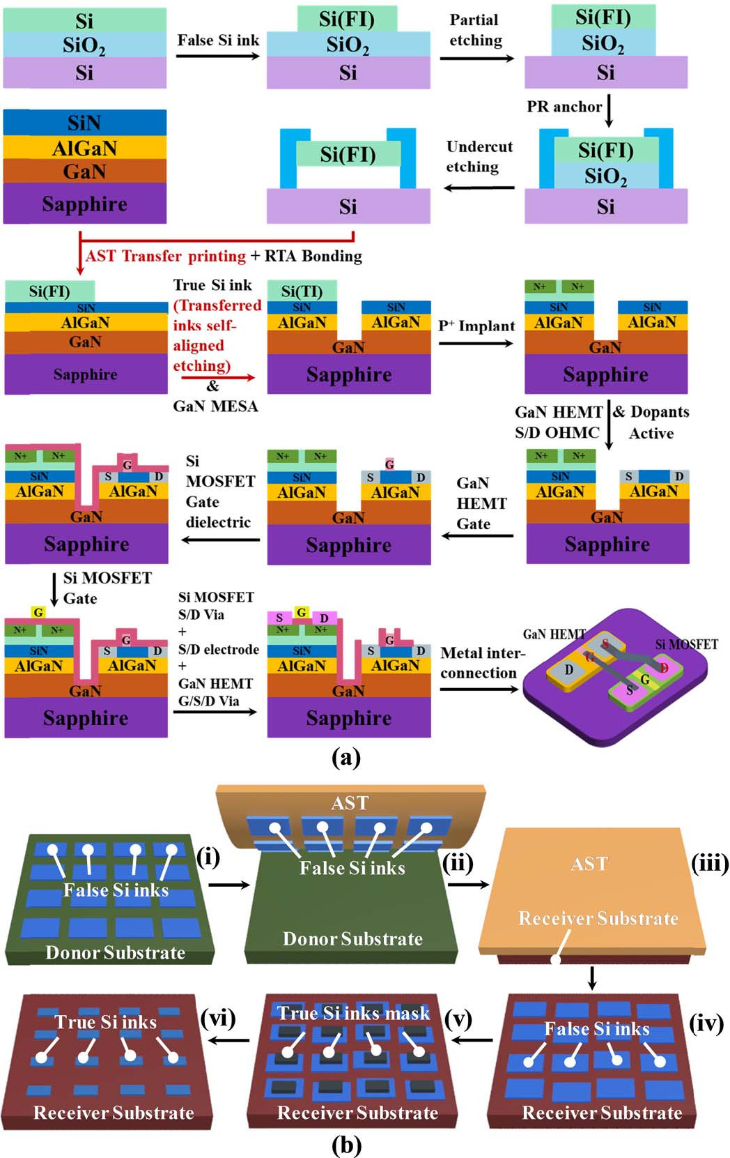
Transfer Printing And Self Aligned Etching For E Mode Gan Transistors
Serena H Eu Downloads 04 Gan Technology Trends Ommic Pdf

Beyond Cmos Heterogeneous Integration Of Iii V Devices Rf Mems And Other Dissimilar Materials Devices With Si Cmos To Create Intelligent Microsystems Philosophical Transactions Of The Royal Society A Mathematical Physical And Engineering

Revisiting The Seminal Apa Optics Gan Hemt Patent Techinsights
Http Www Inrel Npower Eu Sites Default Files T05 Meneghesso Reliability Phd Brixen Jul 17 Pdf
Www Nature Com Articles S 019 3 Pdf Proof T
Mtlsites Mit Edu Users Alamo Pdf 18 Rj 193 paper Pdf
Electronics Free Full Text A Comprehensive Review Of Recent Progress On Gan High Electron Mobility Transistors Devices Fabrication And Reliability Html

Schematic Of The Gate Last Self Aligned Process Flow Download Scientific Diagram

Pdf Qualification Of Wavice Baseline Gan Hemt Process With 0 4 Um Gate On 4 Sic Wafers

Multi Cell Gan Hemt On Single Crystal Diamond

Color Online Flowchart Of Backside Processing Of The Gan Hemt On A Download Scientific Diagram

Micromachines Free Full Text A Novel Gan Metal Insulator Semiconductor High Electron Mobility Transistor Featuring Vertical Gate Structure Html
2
Arxiv Org Pdf 02 029
Electronics Free Full Text A Comprehensive Review Of Recent Progress On Gan High Electron Mobility Transistors Devices Fabrication And Reliability Html
Iopscience Iop Org Article 10 1149 2 jss Pdf

Fabrication Process Flow Of Gan Hemts With T Shape Gates Download Scientific Diagram
Obliterating Dynamic On Resistance Degradation News
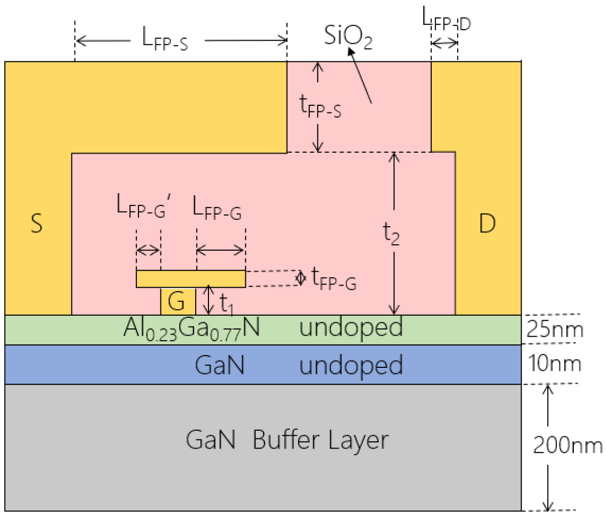
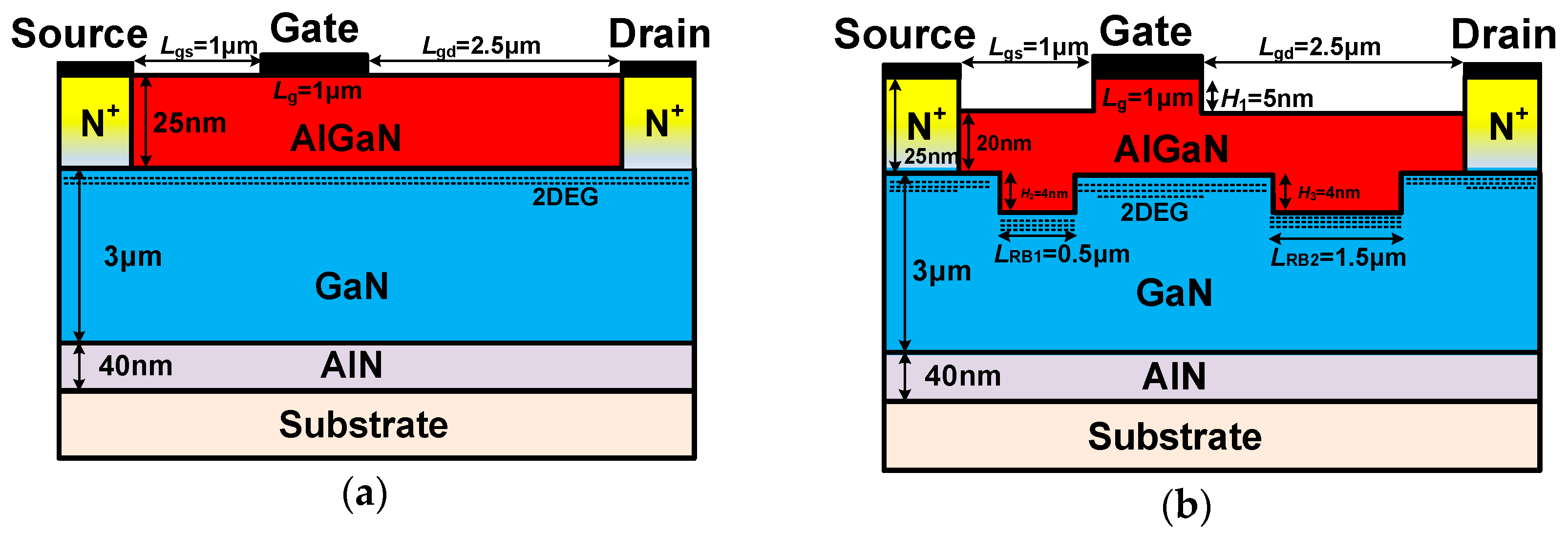
Electronics Free Full Text Simulation Of Algan Gan Hemts Breakdown Voltage Enhancement Using Gate Field Plate Source Field Plate And Drain Field Plate Html
Iopscience Iop Org Article 10 10 1402 46 Ab1438 Pdf
Micromachines Free Full Text Vertical Leakage In Gan On Si Stacks Investigated By A Buffer Decomposition Experiment Html
Snfexfab Stanford Edu Sites G Files Sbiybj8726 F Sections Diplayfiles Engr241 Final Report Sj Al 1819win Pdf
Ieeexplore Ieee Org Iel5 55 Pdf
2
Ieeexplore Ieee Org Iel7 Pdf
Ieeexplore Ieee Org Iel5 16 Pdf
Ieeexplore Ieee Org Iel7 63 Pdf

On The Performance Of Gan On Silicon Silicon Carbide And Diamond Substrates Jarndal International Journal Of Rf And Microwave Computer Aided Engineering Wiley Online Library

Process Flow The Proposed Triple Material Gate N Polar Mos Hemt Download Scientific Diagram
An Aunps Functionalized Algan Gan High Electron Mobility Transistor Sensor For Ultrasensitive Detection Of Tnt Rsc Advances Rsc Publishing

A Reliable And Efficient Small Signal Parameter Extraction Method For Gan Hemts Chen International Journal Of Numerical Modelling Electronic Networks Devices And Fields Wiley Online Library
An Analytical Model For Algan Gan Mos Hemt For High Power Applications Springerlink

Research Ujwal Radhakrishna
Http Www Semiconductor Today Com Features Pdf Semiconductor Today December January Trends Toward Pdf
2
Http Global Sei Com Technology Tr Bn81 Pdf 81 07 Pdf
Icorlab Ece Illinois Edu Files 07 Lee Dissertation Pdf

Figure 2 From Two Dimensional Electron Gas 2deg Idt Saw Devices On Algan Gan Heterostructure Semantic Scholar
Pdf Modeling Of Gan Hemt Devices At High Frequency Bands
Www Systemplus Fr Wp Content Uploads 18 04 Sp165 Gan On Silicon Transistor Comparison Sample 3 Pdf
Www Nature Com Articles S 019 3 Pdf Proof T
Www Systemplus Fr Wp Content Uploads 03 Sp550 Nexperia Aec Q101 Qualified 650 V Gan Based Power Device Sample Pdf
A Sandwich Structured Algan Gan Hemt With Broad Transconductance And High Breakdown Voltage Journal Of Materials Chemistry C Rsc Publishing Doi 10 1039 C9tcg
Iopscience Iop Org Article 10 1149 1 Pdf

Plot Of The Energy Band Profile Of The Vertical Hemt With A P Gan Cbl Download Scientific Diagram

Flowchart For Development Of Large Signal Model Of Algan Gan Hemts Download Scientific Diagram

Em In Situ Em Sin Combined With Etch Stop Barrier Structure For High Frequency Algan Gan Hemt
Www Nature Com Articles S 019 3 Pdf Proof T

Moscap And Hemt Process Flows A Moscap Process Flow N Gan Substrate Download Scientific Diagram
Iopscience Iop Org Article 10 10 1361 6463 af9d Pdf
On The Baliga S Figure Of Merits Bfom Enhancement Of A Novel Gan Nano Pillar Vertical Field Effect Transistor Fet With 2deg Channel And Patterned Substrate Nanoscale Research Letters Full Text

Vertical Gan Devices For A New Power Electronics Power Electronics News
Arxiv Org Pdf 02 029

Pdf Development Of K And Ka Band High Power Amplifier Gan Mmic Fabrication Technology
Www Systemplus Fr Wp Content Uploads 18 04 Sp165 Gan On Silicon Transistor Comparison Sample 3 Pdf
Gan Sic Based High Electron Mobility Transistors For Integrated Microwave And Power Circuits

An Algan Gan Hemt By A Reversed Pyramidal Channel Layer Investigation And Fundamental Physics Sajjadi Jaghargh International Journal Of Numerical Modelling Electronic Networks Devices And Fields Wiley Online Library
Www Systemplus Fr Wp Content Uploads 18 04 Sp165 Gan On Silicon Transistor Comparison Sample 3 Pdf
Gan Sic Based High Electron Mobility Transistors For Integrated Microwave And Power Circuits
S3 I Micronews Com Uploads 11 Sp580 Stmicroelectronics Mastergan1 Half Bridge Driver Sample Pdf

Gan Power Devices The Hemt Youtube
Micromachines Free Full Text Novel High Energy Efficiency Algan Gan Hemt With High Gate And Multi Recessed Buffer Html
Obliterating Dynamic On Resistance Degradation News
Snfexfab Stanford Edu Sites G Files Sbiybj8726 F Sections Diplayfiles Engr241 Final Report Sj Al 1819win Pdf

A Planar Integration Process For E D Mode Algan Gan Hemt Dcfl Integrated Circuits Semantic Scholar
2
Electronics Free Full Text A Comprehensive Review Of Recent Progress On Gan High Electron Mobility Transistors Devices Fabrication And Reliability Html
Iopscience Iop Org Article 10 10 1361 6463 af9d Pdf
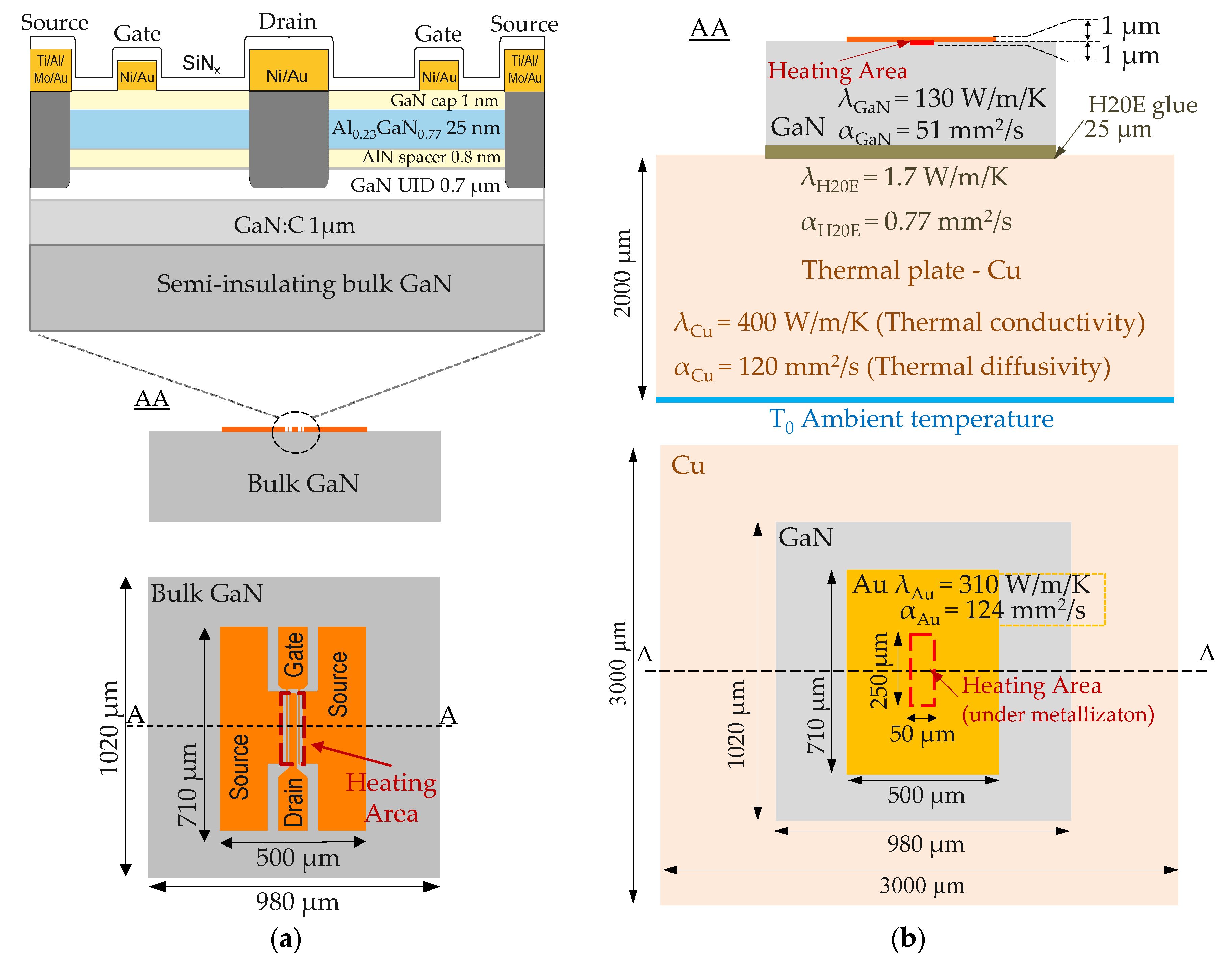
Electronics Free Full Text Characterization Of Self Heating Process In Gan Based Hemts Html
Aip Scitation Org Doi Pdf 10 1063 1


